
U.S. Semiconductor R&D USD 874,000,000: 7 Companies Selected for Support and the Impact on South Korea
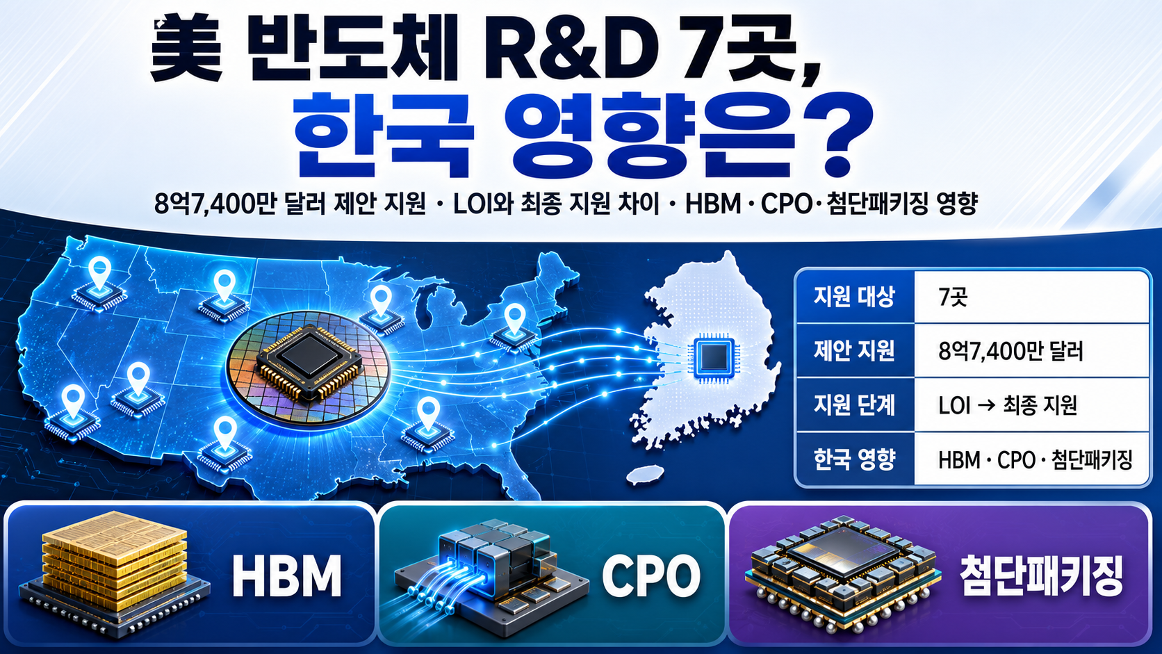
This article is based on the latest available news reports and official materials verified as of 2026-08-01 Korea Standard Time.
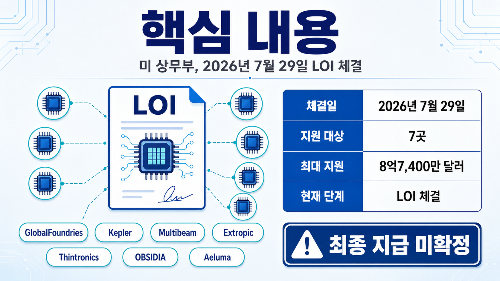
The U.S. Department of Commerce signed letters of intent on 2026-07-29 local time to provide up to USD 874,000,000 in funding to 7 semiconductor R&D companies. The recipients are GlobalFoundries, Kepler, Multibeam, Extropic, Thintronics, OBSIDIA Semiconductors, and Aeluma. Final disbursements have not yet been confirmed.
For South Korea, the more important variable is not an immediate change in HBM sales but the development of U.S.-based supply chains for next-generation AI memory, CPO, and advanced packaging materials and equipment.
What Was Announced in the U.S. Semiconductor R&D Funding Initiative?
The announcement concerns the signing of letters of intent, or LOIs, to provide a total of 8 hundred million USD 74,000,000 in federal incentives to 7 companies under the U.S. CHIPS and Science Act.
An LOI outlines the proposed funding direction and maximum amount. Final funding agreements can be signed only after additional due diligence, negotiations, business plan reviews, and approval of detailed terms by the U.S. Department of Commerce.
The key conditions confirmed so far are as follows.
Announcement date: 2026-07-29, U.S. local time
Total proposed funding: Up to 8 hundred million USD 74,000,000
Recipients: 7 companies
Supported fields: Silicon photonics, AI memory, computing architectures, advanced packaging, substrate and insulating materials, and semiconductor security
Current status: Letters of intent signed, not final disbursements
Additional condition: Upon finalization of the funding, the U.S. government is expected to acquire a minority, noncontrolling equity stake in each company
Therefore, even if headlines describe the funding as confirmed, it is important to distinguish that characterization from the actual status, in which final company-specific agreements and project milestones remain outstanding.
The 7 Recipients and Their Maximum Funding Amounts
| Company | Maximum Funding | Share of Total | Development Focus | Related South Korean Industries |
|---|---|---|---|---|
| GlobalFoundries | USD 300,000,000 | 34.3% | Silicon photonics and CPO | Foundries, photonic semiconductors, AI packaging |
| Kepler | USD 245,000,000 | 28.0% | 3D and ferroelectric-based AI memory | HBM, PIM, next-generation memory |
| Multibeam Corporation | USD 140,000,000 | 16.0% | Fine-pitch advanced packaging technology | 2.5D and 3D packaging, equipment |
| Extropic | USD 75,000,000 | 8.6% | Thermodynamic sampling processors | Low-power AI semiconductors, mature process nodes |
| Thintronics | USD 50,000,000 | 5.7% | Ultra-low-loss interlayer dielectric materials | Package substrates, materials |
| OBSIDIA Semiconductors | USD 34,000,000 | 3.9% | Nondestructive identification of counterfeit and malicious components | Supply chain authentication, semiconductor security |
| Aeluma | USD 30,000,000 | 3.4% | Large-diameter photonic semiconductor substrates that do not use indium phosphide | Photodetectors, lasers, optical interconnects |
| Total | USD 874,000,000 | 100% |
The shares were calculated using 'maximum funding per company ÷ USD 874,000,000 × 100.' These are the author's calculations, rounded at the second decimal place.
The combined allocation to the top 3 companies, GlobalFoundries, Kepler, and Multibeam, is USD 685,000,000. This means approximately 78.4% of the total funding is concentrated in three areas: optical interconnects, AI memory, and advanced packaging.
Why Is GlobalFoundries Receiving the Largest Allocation of USD 300,000,000?
GlobalFoundries has been allocated up to USD 300,000,000 to develop co-packaged optics, or CPO, a technology that places optical components close to AI processors.
CPO uses light instead of electrical signals to transmit data between chips. It is attracting attention as a way to reduce power consumption, heat generation, and transmission-distance limitations as data traffic increases in AI servers.
Through this funding, the U.S. government aims to accelerate GlobalFoundries' CPO research and development schedule by 2–3 years compared with its original plan. The company has stated that its next-generation technology targets transmission speeds of approximately 400Gbps per channel and energy-efficiency improvements of up to 5 times compared with existing implementations.
However, these figures are company-stated development targets, not independently verified performance results from mass-produced products.
Will Kepler's AI Memory Replace HBM?
Kepler has been allocated up to USD 245,000,000 to develop high-performance AI memory combining 3-dimensional structures with ferroelectric technology.
Ferroelectric memory stores data using the polarization states of materials. It may reduce the latency and power consumption caused by repeatedly transferring data between processors and memory.
Kepler's allocation accounts for 28.0% of the total, making it the second largest. This can be interpreted as a sign that the United States views memory bottlenecks, rather than GPU computing performance alone, as a strategic issue.
However, Kepler has not yet disclosed sufficient details about product specifications, customers, production capacity, mass-production schedules, or performance comparisons with HBM. At this stage, there is insufficient evidence to conclude that its technology will directly replace the HBM products of Samsung Electronics and SK hynix.
Even if commercialization succeeds, the technology may initially complement HBM and DRAM in specific inference workloads or in-memory computing applications rather than replacing HBM entirely.
How Could Multibeam and Thintronics Transform Advanced Packaging?
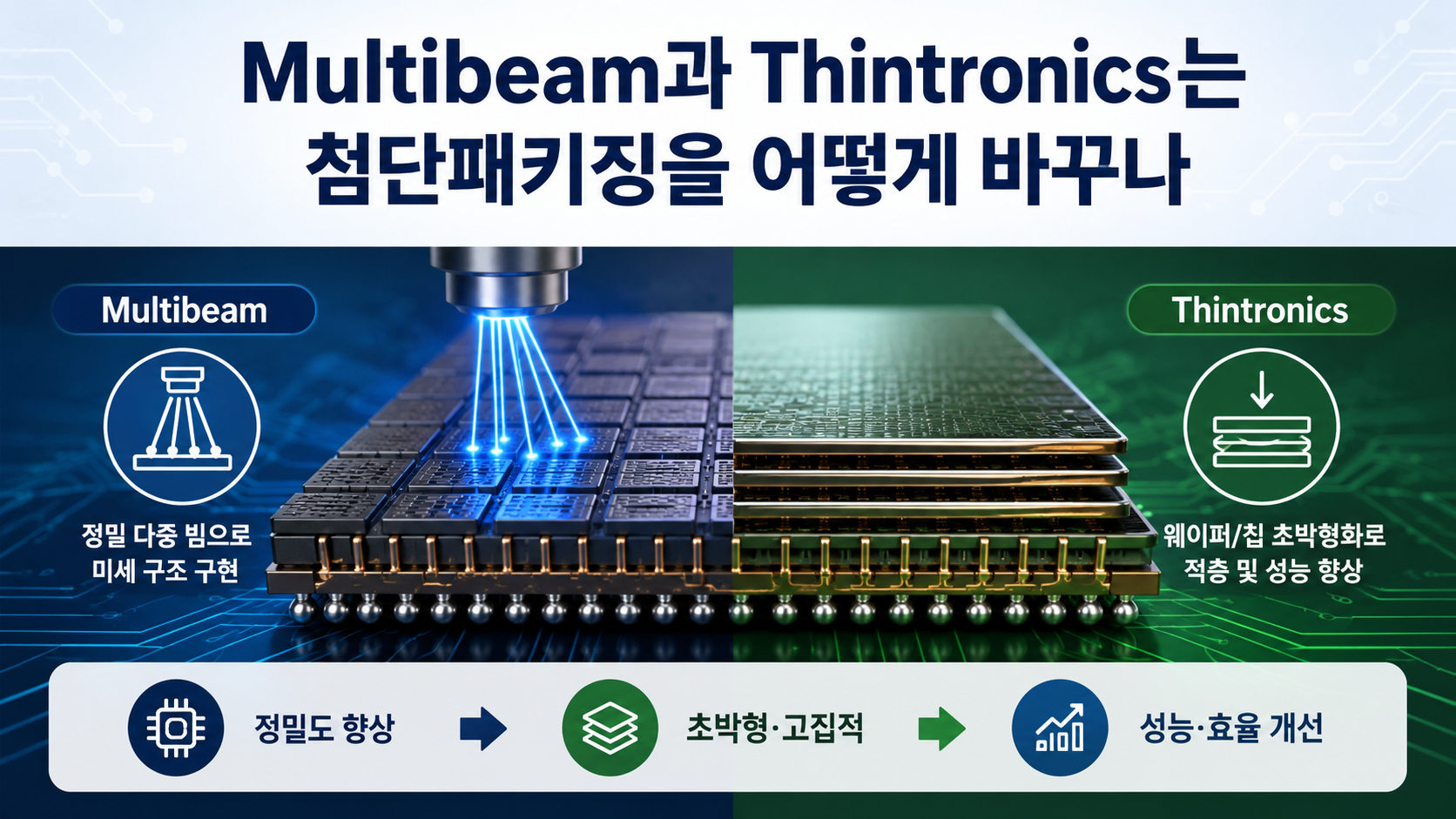
Multibeam has been allocated up to USD 140,000,000 to develop advanced packaging technology that stacks multiple chips and connects them through thousands of fine interconnections.
The company's core technology uses multiple electron beams to write circuit patterns directly without masks. Its goal is to produce fine patterns rapidly for chiplets and 2.5D and 3D packaging, which combine different chips into a single package.
Thintronics has been allocated up to USD 50,000,000 to develop ultra-low-loss interlayer dielectric materials that reduce high-speed signal losses inside semiconductor packages.
The combined funding for the two companies is USD 190,000,000, representing approximately 21.7% of the total. The United States appears to be pursuing not only additional packaging factories but also the fine-patterning equipment and substrate materials needed to support them.
For South Korean companies producing package substrates, insulating materials, and plating and etching equipment, this creates both competition and opportunities. Competition could intensify if U.S. alternatives pass customer qualification tests, but Korean suppliers may also gain opportunities to participate as U.S.-based manufacturing partners or joint development suppliers.
The Roles of Extropic, OBSIDIA, and Aeluma
Extropic
Extropic is developing a thermodynamic sampling unit, or TSU, that uses natural thermal fluctuations to solve probabilistic problems.
Its goal is to process probability-intensive workloads, including generative AI, optimization, and simulation, with less energy than conventional GPUs. The company emphasizes that its technology can also be manufactured using mature process nodes rather than the most advanced semiconductor fabrication processes.
However, claims that the technology could achieve energy efficiency orders of magnitude better than conventional GPUs represent the company's stated objectives. Its actual competitiveness must be assessed by examining the throughput, accuracy, software compatibility, and total system deployment costs of mass-produced chips.
OBSIDIA Semiconductors
OBSIDIA Semiconductors is developing technology to identify counterfeit and malicious semiconductor components without destroying or disassembling them.
The technology is intended to verify the origin of chips and detect modifications in AI data centers and defense and aerospace supply chains. If requirements for chip traceability, authenticity verification, and manufacturing data submissions become stricter in U.S. government procurement, South Korean exporters may also need to establish corresponding systems.
Aeluma
Aeluma is developing large-diameter substrate technology that does not use InP to reduce supply constraints associated with conventional indium phosphide, or InP, substrates.
These substrates could be used to manufacture high-speed photodetectors and lasers for optical communications in AI data centers. Viewed alongside GlobalFoundries' CPO initiative, Aeluma's project illustrates the U.S. effort to build an interconnected supply chain spanning photonic semiconductor components, substrates, and packaging.
Under the author's classification, the combined optical and photonics-related funding for GlobalFoundries and Aeluma is USD 330,000,000. This represents approximately 37.8% of the total, making it one of the largest technological priorities in the funding initiative.
What Does This Mean for South Korea's Semiconductor Industry?
This funding initiative will not directly change the short-term earnings of Samsung Electronics or SK hynix. All 7 awards remain at the R&D letter-of-intent stage, and neither mass-production timelines nor customer orders have been disclosed.
Over the medium to long term, the important development is the emergence of alternative U.S.-based supply chains in areas surrounding AI memory and advanced packaging, where South Korea has established strengths.
| Area of Impact | Short-Term Impact | Medium- to Long-Term Impact | Indicators to Monitor |
|---|---|---|---|
| HBM and AI memory | Limited impact | Potential changes in memory architectures if ferroelectric and 3D memory are commercialized | Kepler prototypes, performance versus HBM, customers |
| CPO and silicon photonics | Intensifying R&D competition | Stronger U.S. photonic semiconductor supply chain | GlobalFoundries mass-production schedule, optical module partners |
| Advanced packaging | Limited immediate revenue impact | Broader customer qualification of U.S. equipment and materials | Multibeam throughput, Thintronics material qualification |
| Semiconductor security | New standards under consideration | Potentially stricter traceability requirements in U.S. government procurement and defense | Supply chain authentication standards, inspection data requirements |
| Low-power AI chips | Early-stage technology validation | Diversification of AI computing approaches beyond GPUs | Extropic benchmarks, software ecosystem |
SK hynix is expanding its AI memory portfolio, including HBM4 and HBM4E, in 2026. Samsung Electronics is also pursuing an AI semiconductor strategy connecting foundry services, advanced packaging, and CPO, alongside its HBM4 supply partnerships.
Therefore, this U.S. funding initiative is not an investment in niche technologies unrelated to South Korea. It directly intersects with HBM, next-generation memory, CPO, and advanced packaging, all areas in which South Korea is either a leader or actively developing capabilities.
What South Korean Companies Should Check Now
1. Whether Final Funding Agreements Are Signed
Companies should not assume that the amounts announced in the LOIs will be disbursed unchanged. They need to verify the final contract amounts, government equity conditions, required company contributions, project milestones, and payment schedules.
2. Manufacturing Partners and Customers
The foundries with which R&D companies sign manufacturing agreements, and the AI accelerator and data center companies that test their products, will be decisive indicators of commercial viability.
The potential participation of South Korean companies should also be assessed only after final suppliers and joint development partners are disclosed.
3. Verified Results Rather Than Technology Targets
For transmission speeds, power efficiency, memory bandwidth, and packaging throughput, companies must distinguish between corporate performance targets and verification results from independent organizations or customers.
Successful prototypes and economically viable mass production are also different stages of development.
4. U.S. Manufacturing and Security Requirements
Because the funding is premised on research, development, and production in the United States, additional conditions may apply concerning domestic production ratios, country of origin, technology security, and supply chain traceability.
South Korean materials, parts, and equipment suppliers should review in advance the production-history records, authenticity verification systems, and data management standards they may need when supplying U.S. customers.
5. Overlaps and Gaps in Domestic R&D
South Korea is also implementing new semiconductor R&D and advanced packaging support programs in 2026. Comparing these programs with the U.S. funding priorities can help determine whether CPO materials, ferroelectric AI memory, ultra-low-loss dielectric materials, and chip authentication technologies are sufficiently integrated within South Korea's domestic technology ecosystem.
Points to Consider Before Making Investment Decisions
USD 874,000,000 does not represent revenue already generated or confirmed corporate valuations. It is the sum of the maximum potential funding amounts for the individual companies.
Technology and financial information is particularly limited for privately held startups. An announced letter of intent alone does not establish technological success, customer acquisition, or mass-production revenue.
When evaluating listed companies and related South Korean stocks, investors should distinguish claims of 'benefiting from U.S. funding' from verified developments such as actual supply agreements, customer qualifications, equipment orders, and product revenue.
Information That Has Not Yet Been Disclosed
As of 2026-08-01, the following details have not been sufficiently disclosed through official sources.
Dates when final funding agreements will be signed for each company
Actual disbursement amounts and annual payment schedules
The equity percentage the U.S. government will acquire in each company
Details of Kepler's memory architecture and mass-production schedule
Manufacturing partners and major customers across the projects
Independently verified performance results for each technology
Supply agreements or joint development projects involving South Korean companies
The scope of export controls and procurement conditions applicable after funding
When new announcements are made, updates should cover not only funding amounts and technology descriptions but also the tables, implications for South Korea, and FAQ section.
Frequently Asked Questions
Which 7 Companies Were Selected for U.S. Semiconductor R&D Funding?
GlobalFoundries, Kepler, Multibeam Corporation, Extropic, Thintronics, OBSIDIA Semiconductors, and Aeluma.
Has the Entire USD 874,000,000 Already Been Disbursed?
No. The figure represents the combined maximum potential funding amounts specified in the 7 letters of intent. Final agreements and project milestone reviews are still pending.
Which Company Is Receiving the Largest Allocation?
GlobalFoundries has the largest allocation, at up to USD 300,000,000. This represents approximately 34.3% of the total and is intended for CPO and silicon photonics development.
Could Kepler's AI Memory Replace HBM?
It is difficult to determine based on currently available information. The technology could become a long-term competitor, but it may initially complement HBM in certain AI computing workloads.
Is This Immediately Bad News for South Korean Companies?
It is difficult to characterize the announcement as an immediate negative development. The projects remain at the R&D letter-of-intent stage, with no confirmed mass production or customer orders. However, the simultaneous U.S. effort to develop memory, optical, and packaging supply chains represents a medium- to long-term competitive factor.
What Announcements Should Be Monitored Next?
The next developments to watch are final company-specific funding agreements, technology milestones, manufacturing partners, customers, mass-production schedules, and U.S. domestic supply chain requirements.