

Will SK hynix's Indiana HBM Be Made in the USA? How Korean Wafer Production and U.S. Packaging Work Together
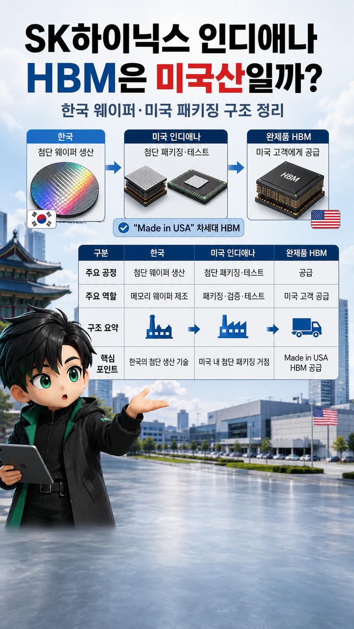
The HBM that SK hynix plans to manufacture in Indiana will not be produced entirely in the United States from start to finish. Instead, advanced wafers will be manufactured in South Korea and shipped to Indiana, where they will undergo advanced packaging and testing to become finished HBM products. SK hynix describes these products as next-generation 'Made in USA' HBM intended for American customers.
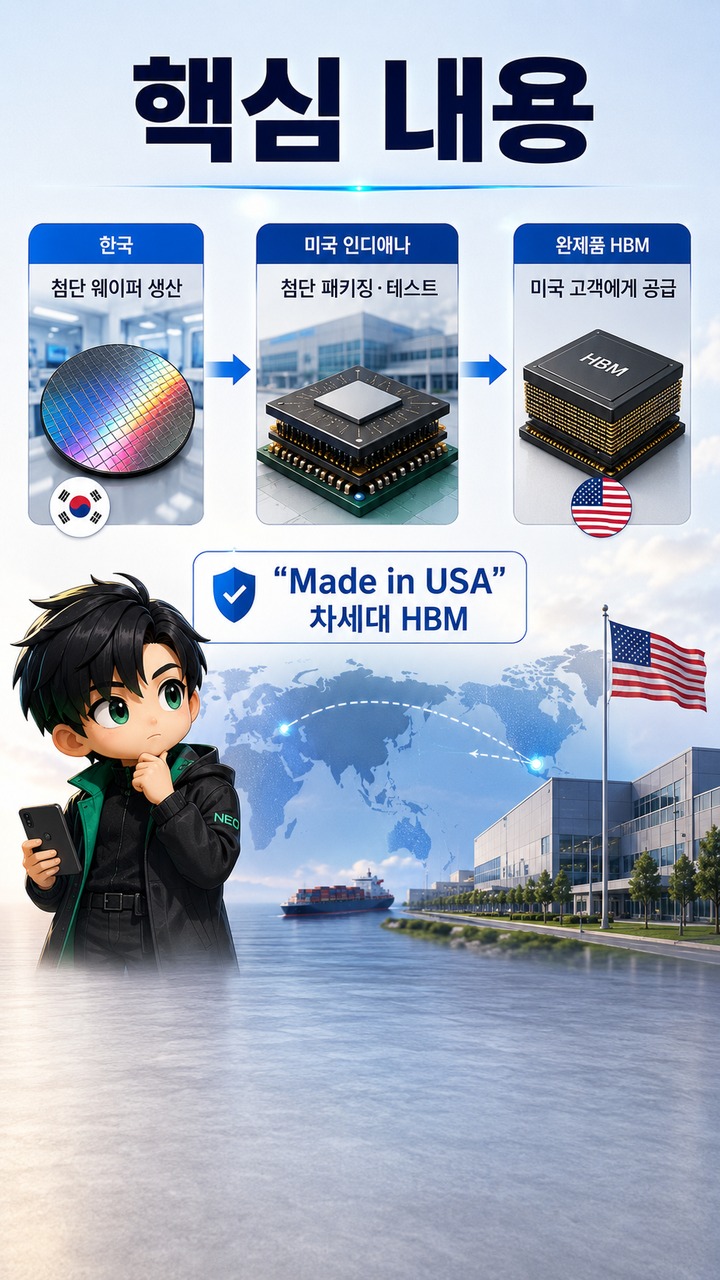
As of 2026-08-28, the Indiana facility is targeting a cleanroom opening in October 2028 and mass production of next-generation HBM in the second half of 2029. This raises two questions: Why is it called a U.S. HBM production base if the wafers are manufactured in South Korea, and which manufacturing processes will the Indiana facility actually handle?
HBM Will Not Be Manufactured Entirely From Scratch in Indiana
Semiconductor manufacturing can broadly be divided into front-end processing, which creates circuits on wafers, and back-end processing, which connects, stacks, and tests fabricated chips to turn them into finished products.
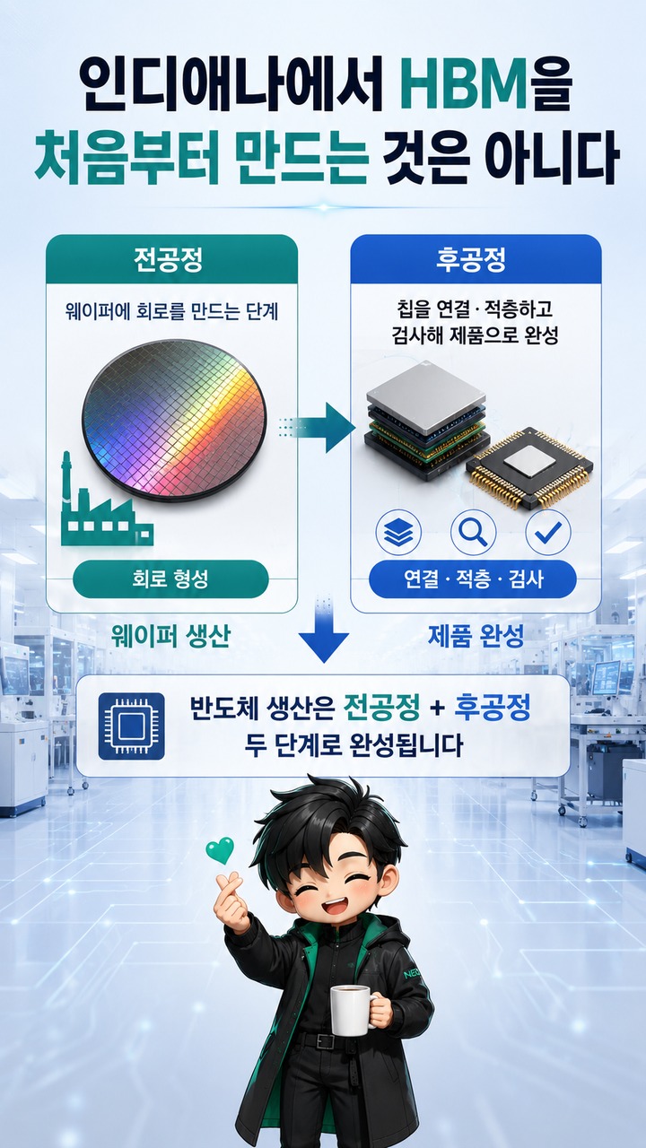
The Indiana production structure announced by SK hynix is as follows.
South Korean production facilities
→ Manufacture advanced DRAM wafers
Indiana, United States
→ Advanced HBM packaging using wafers and chips
→ Testing and performance validation
→ Research and development of next-generation packaging technologies
U.S. customers
→ Delivery of finished HBM products
In its official announcement, SK hynix also stated that advanced wafers manufactured in South Korea would be shipped to Indiana for advanced packaging and testing before being supplied to U.S. customers.
This is therefore different from a scenario in which South Korean production facilities disappear and HBM manufacturing moves entirely to the United States. It is better understood as a division of manufacturing responsibilities linking wafer production in South Korea with advanced packaging in the United States.
Why Is Packaging So Important for HBM?
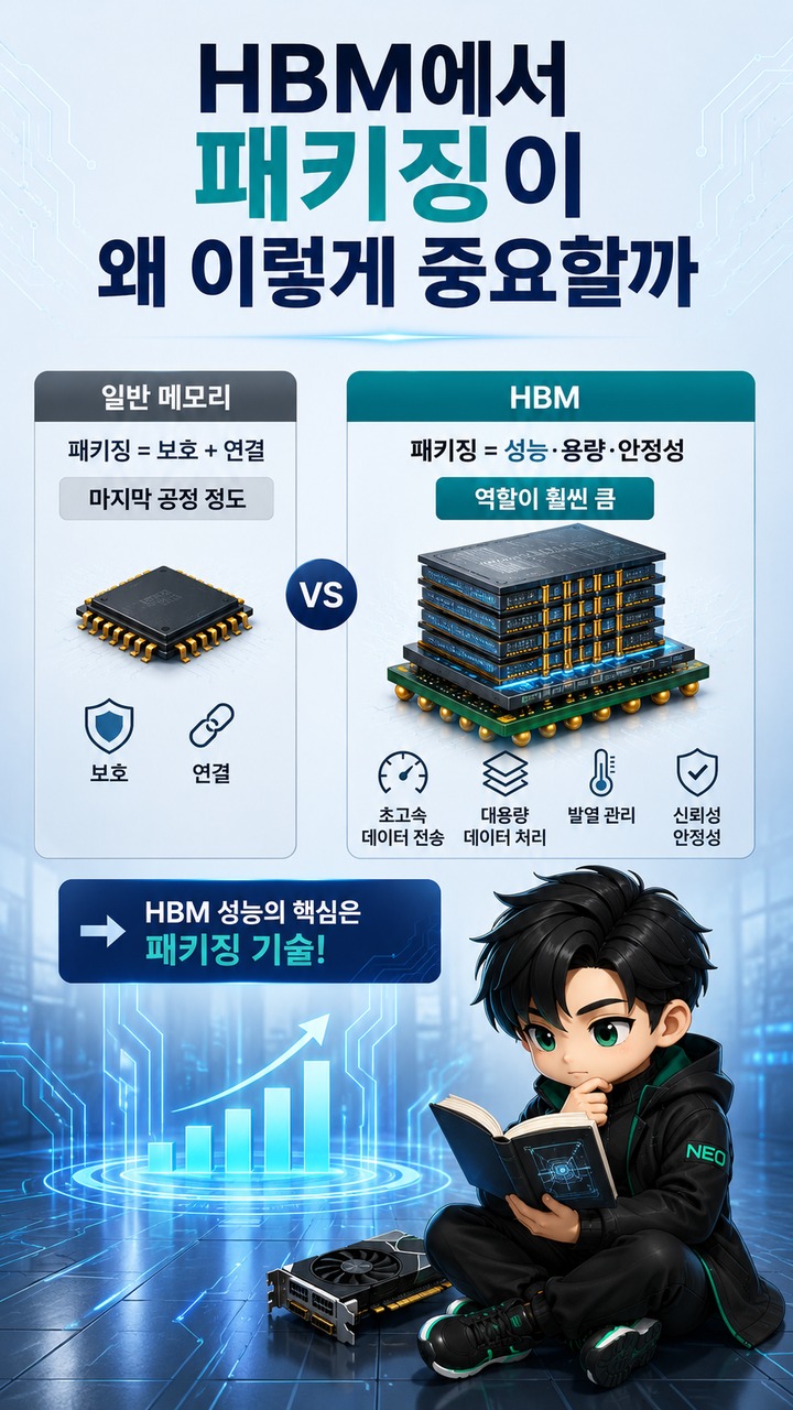
In conventional memory manufacturing, packaging may seem like little more than the final step that protects a chip and connects it to external components. In HBM, however, packaging plays a much greater role.
HBM is a type of memory that vertically stacks multiple DRAM chips to transfer large amounts of data at high speeds. Technologies such as through-silicon vias (TSVs) are used to connect the chips, while packaging technology affects the integrity of connections between stacked chips, heat dissipation, power efficiency, and manufacturing yield. SK hynix describes TSV as a core HBM technology that creates microscopic holes in DRAM chips and connects them vertically using electrodes.
AI accelerators do not necessarily become faster simply because their computing performance improves. If data cannot move quickly enough between the GPU and memory, a bottleneck develops.
Advanced packaging helps reduce the distance data must travel by connecting processors, HBM, and other chips at high density and in close proximity. This is why interconnection technology becomes increasingly important as AI semiconductor performance improves.
In other words, HBM requires a combination of:
Technology for manufacturing high-quality DRAM + technology for precisely stacking multiple DRAM chips + technology for creating reliable connections + technology for controlling heat.
That is why describing the Indiana facility as merely a chip packaging plant would significantly understate its actual role.
Why Build an Advanced Packaging Facility in the United States?
The most important feature of the project is the establishment of an HBM manufacturing and research base close to major U.S. AI customers.
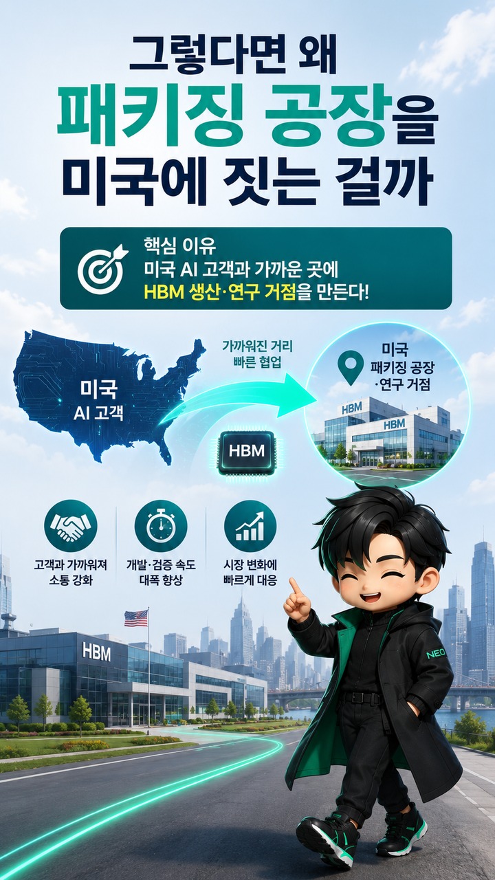
SK hynix plans to make the Indiana facility its first HBM production base in the United States and establish an 'Advanced Packaging R&D Testbed' alongside its production lines.
The proposed facility will support collaborative research into next-generation packaging technologies involving SK hynix, customers, universities, and partner companies, extending to prototype development and performance validation. Research and development collaboration with Purdue University in advanced packaging is also planned.
HBM is a product whose performance requirements evolve rapidly alongside advances in AI accelerators.
Recently, the industry has been moving beyond supplying identical specifications to every customer, with custom HBM tailored to AI chip architectures and power and thermal requirements becoming increasingly important. SK hynix has also identified HBM4E and customer-specific HBM as major directions following HBM4.
Locating packaging and R&D facilities close to customers is therefore significant not merely because it shortens logistics distances, but because it can accelerate collaborative product development and validation.
Will HBM4E Also Be Manufactured in Indiana?
It is important to distinguish between the different timelines.
SK hynix announced that it had already supplied samples of 12-layer HBM4E to major customers in June 2026. The product was developed with targets of speeds of up to 16Gbps per pin and power efficiency improvements of at least 20% compared with HBM4.
By contrast, the Indiana facility is targeting full-scale mass production in the second half of 2029.
Rather than identifying one specific HBM generation, SK hynix's official announcement describes the products to be manufactured in Indiana more broadly as 'next-generation HBM.'
Some recent reports have identified HBM4E as a product expected to enter mass production in Indiana in 2029. However, the product roadmap could change depending on customer qualification and the pace of transitions between HBM generations.
At this stage, therefore, it is more appropriate to view the Indiana facility not as a plant dedicated exclusively to one HBM generation, but as a long-term U.S. manufacturing base for next-generation HBM packaging and research and development from 2029 onward.
Is South Korea's HBM Production Moving to the United States?
Based on currently disclosed plans, that interpretation is difficult to support.
In fact, SK hynix has explicitly outlined a production structure connecting its South Korean manufacturing facilities with its Indiana plant.
Because wafers will be manufactured in South Korea and packaged in the United States, South Korea's front-end manufacturing capacity will remain essential.
SK hynix is also expanding its domestic manufacturing infrastructure for next-generation DRAM and HBM while simultaneously increasing investments in packaging. The company describes its Yongin Semiconductor Cluster, Cheongju manufacturing facilities, and advanced packaging facility in Indiana as parts of an interconnected AI memory production system.
In simplified terms, the structure can be understood as follows:
South Korea = Core wafer manufacturing baseUnited States = Advanced packaging, testing, R&D, and a production base close to customers
Rather than one manufacturing base completely replacing the other, the two will operate as interconnected parts of the production system.
What Should Investors Monitor at the Indiana Fab?
Even with an investment exceeding USD 4,000,000,000, the start of factory construction does not automatically translate into higher revenue or profits.
Several milestones remain before the project's actual business impact can be assessed.
First, investors should check whether the cleanroom construction schedule targeting October 2028 is progressing as planned. Equipment installation, process stabilization, and customer qualification must then follow before mass production can begin in the second half of 2029.
Another important factor is demand for next-generation HBM, not simply production volume.
Because HBM is a critical memory component in AI accelerators, new product launches by AI chipmakers such as Nvidia, the pace of data center investment, and HBM adoption volumes among individual customers could all affect SK hynix's financial performance.
Large-scale factory investments also create depreciation expenses and initial operating costs. Rather than assuming that 'building a U.S. factory = a rising share price,' investors need to consider HBM sales volumes, pricing, manufacturing yields, customer qualification, capital expenditure burdens, and actual facility utilization rates together.
The Key Is Completing HBM Manufacturing in the United States, Not Producing Wafers There
The most important point to understand about SK hynix's Indiana fab is this:
The core DRAM wafers used in HBM will be manufactured in South Korea, while the chips will undergo advanced packaging and testing in the United States to become finished HBM products.
However, packaging in HBM is not merely a finishing step. It is one of the core technologies that determine performance, thermal behavior, power efficiency, and product reliability by precisely stacking and connecting multiple DRAM chips.
The significance of the Indiana facility should therefore be assessed not only in terms of increased production capacity, but also in terms of the creation of an HBM manufacturing system that connects South Korea's memory manufacturing expertise with U.S. AI customers and the American research and development ecosystem.
Related Articles
Why Does Nvidia's Gross Margin of 75% Matter? How to Interpret Margins in Earnings Reports