

SK hynix Breaks Ground on Indiana Fab: What Has Changed in the KRW 4,000,000,000,000-Scale Investment and 2029 HBM Mass Production Timeline?
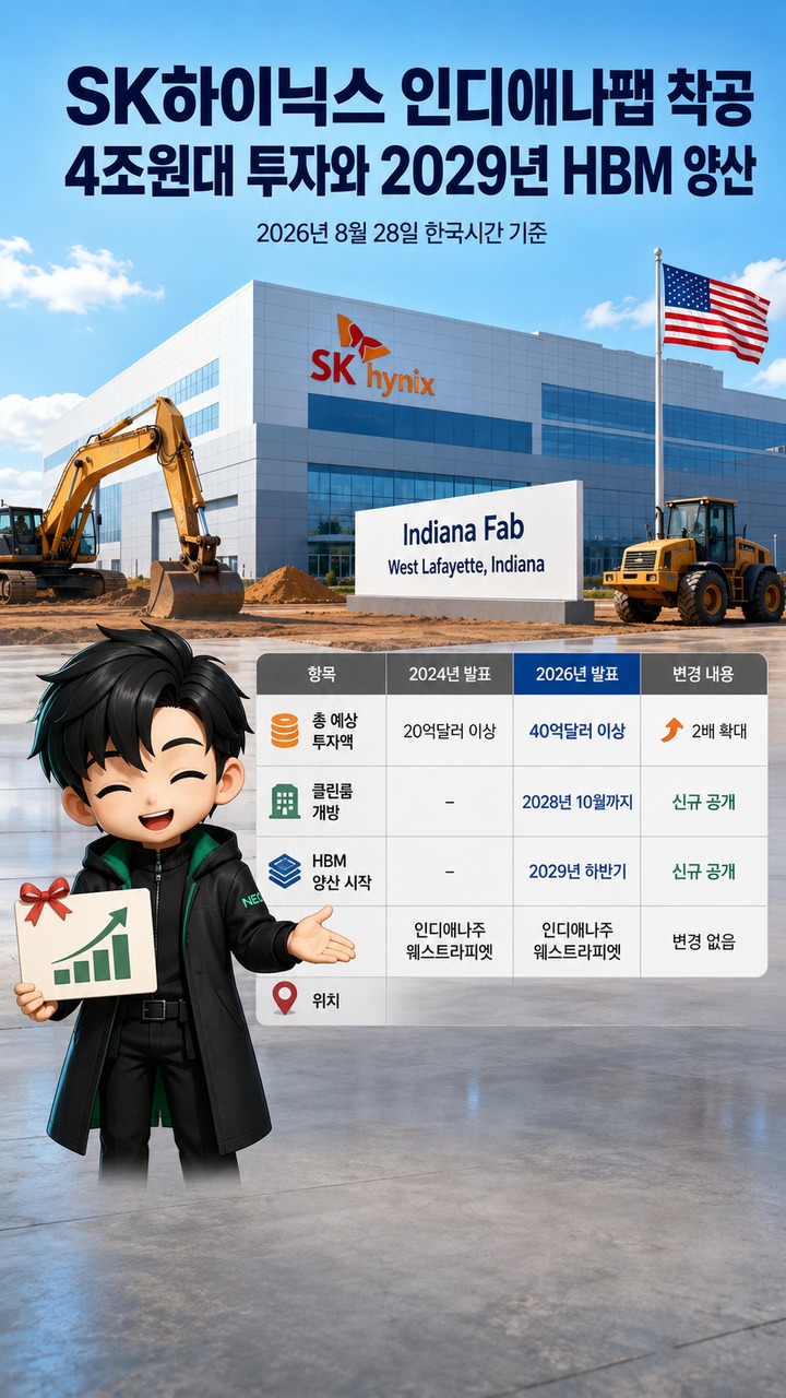
SK hynix held a groundbreaking ceremony for an advanced packaging facility for AI memory in West Lafayette, Indiana, USA. As of 2026-08-28 Korea time, the company's total projected investment is more than USD 4,000,000,000, with cleanrooms scheduled to open by October 2028 and mass production of next-generation HBM targeted to begin in the second half of 2029. It is also important to note that the current schedule has been pushed back from the original plan, announced in 2024, to begin mass production in the second half of 2028.
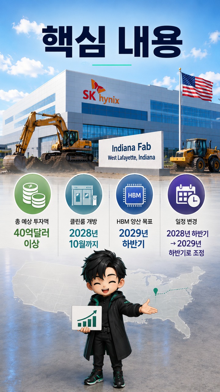
This project is somewhat different from simply adding another semiconductor factory in the United States. Advanced wafers manufactured in South Korea will be shipped to the United States for packaging and testing. Alongside the production line, the facility will also include an R&D testbed for developing next-generation packaging technologies and validating prototypes.
What Will the Indiana Fab Actually Produce?
The Indiana fab's primary role will be advanced packaging and testing of HBM for AI applications. HBM is high-performance memory that stacks multiple DRAM dies vertically to increase data-processing bandwidth, making it an important component of AI accelerators.
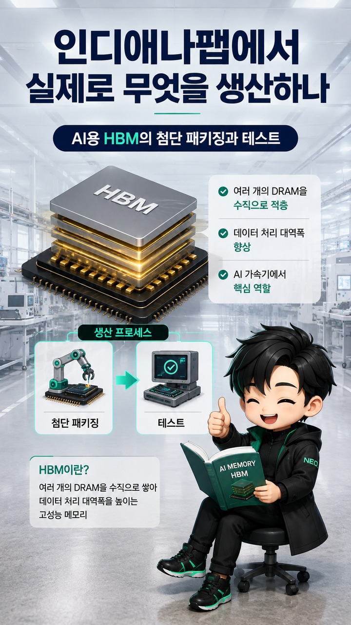
According to the production structure disclosed by SK hynix, the facility will not perform every manufacturing process, starting with wafer fabrication, in the United States. Instead, advanced wafers will be manufactured in South Korea, shipped to the Indiana facility, and then undergo advanced packaging and testing locally before being supplied to U.S. customers.
Advanced packaging refers to back-end semiconductor processes that connect multiple chips within a single package or stack them vertically to improve performance. As it becomes increasingly difficult to achieve performance gains through chip miniaturization alone, packaging technology is also becoming more important for high-performance AI memory.
SK hynix describes the facility as its first HBM production base in the United States. Purdue University has also explicitly identified the project as SK hynix's first U.S. HBM production hub.
Which HBM Product Is Planned for 2029?

The most specific product plan disclosed so far is HBM4E. SK hynix CEO Kwak Noh-jung stated in Indiana that the company plans to begin mass production of next-generation HBM4E in the 3 quarter of 2029.
Rather than identifying a specific product, the company's official announcement stated that mass production of next-generation HBM at the Indiana fab will begin in the second half of 2029. Taken together, these statements indicate that the overall production timeline currently targets the second half of 2029, while the more specific target disclosed at the event is the 3 quarter of 2029.
A figure was also provided for production capacity. CEO Kwak said annual production capacity is expected to reach hundreds of thousands of wafers in terms of wafer input.
However, the 2029 production plan is still approximately 3 years away. SK hynix also explicitly stated in its official announcement that the projected figures and future schedules are forward-looking information and may differ from actual results. Therefore, subsequent announcements will need to be checked for updates on cleanroom openings, equipment installation, and preparations for mass production.
How Has the Timeline Changed Compared With the Original Plan?
The most noticeable change concerns the start of mass production. When SK hynix first officially announced its Indiana investment plan in April 2024, it planned to begin mass production in the second half of 2028.
At the August 2026 groundbreaking announcement, the company presented a schedule under which cleanrooms would open by October 2028, while actual mass production of next-generation HBM would begin in the second half of 2029.
A straightforward comparison of the official announcements is as follows.
April 2024 announcement: Mass production planned for the second half of 2028
August 2026 groundbreaking announcement: Cleanrooms scheduled to open by October 2028
Current mass production target: Second half of 2029
HBM4E target disclosed at the event: Mass production in the 3 quarter of 2029
Comparing the original plan with the latest announcement, the targeted start of mass production has moved back by approximately 1 years. However, SK hynix did not separately specify the reasons for the schedule change in its latest groundbreaking announcement, making it difficult to attribute the delay to any particular factor.
The way the investment amount is described has also changed. In its initial announcement in 2024, the company estimated total investment at 38 hundred million and 7 ten million dollars, whereas at the latest groundbreaking ceremony, it described the amount as more than USD 4,000,000,000.
This does not mean that the final investment amount has been fixed at USD 4,000,000,000. Because the currently disclosed figure is explicitly described as 'more than USD 4,000,000,000,' actual expenditures may change as construction progresses.
What Makes the Research Facility Being Developed With Purdue University Different?
An Advanced Packaging R&D Testbed is planned alongside the production line. Rather than being a facility dedicated solely to mass-produced products, this space is designed to allow customers, universities, and business partners to collaborate on developing next-generation packaging technologies, producing prototypes, and validating performance.
At the groundbreaking ceremony, SK hynix and Purdue University also signed an agreement on R&D cooperation in advanced packaging. The two organizations agreed to expand collaboration toward joint research on system integration, including HBM, and advanced packaging technologies.
Purdue University also has separate infrastructure for semiconductor research. According to the university, its Birck Nanotechnology Center operates approximately 3 ten-thousand plus 3 thousand square feet of specialized research laboratories, along with a large university cleanroom.
This also helps explain why the Indiana facility will place production and R&D functions together. The project aims to establish an environment within the same region where newly developed packaging technologies can progress from research to prototype production and performance validation.
How Large Will the Indiana Fab's Workforce and Supply Chain Be?
SK hynix expects approximately 1,000 employees to work at the Indiana fab itself once the facility enters commercial production. Purdue University has likewise stated that the West Lafayette facility will support approximately 1,000 jobs once production begins.
In addition, the company expects approximately 7,000 direct and indirect jobs to be created through cooperation with local and other U.S. companies during factory construction and commercial operations.
The supply chain will not be limited to the factory itself. SK hynix said it is currently evaluating more than 100 companies as potential suppliers of materials, components, equipment, and other products for the West Lafayette facility.
In other words, the currently disclosed figures of approximately 1,000 fab employees and approximately 7,000 direct and indirect jobs should not be treated as equivalent categories and simply added together. The 1,000 figure represents the fab's workforce during commercial operations, while the 7,000 figure represents projected direct and indirect employment associated with construction and future operations, including jobs at local and other U.S. companies.
What Should Be Monitored After the Groundbreaking?
More important than the groundbreaking ceremony itself is whether the actual production schedule proceeds as planned. The first major milestone to monitor is the opening of cleanrooms scheduled by October 2028.
Cleanrooms are essential spaces where semiconductor manufacturing and packaging equipment is installed and controlled production environments are established. After the cleanrooms are ready, equipment installation, process setup, trial production, and other stages must be completed before the facility can achieve its mass production target for the second half of 2029.
The second area to watch is the product roadmap. Although a target of mass-producing HBM4E in the 3 quarter of 2029 was disclosed at the event, further announcements will be needed to clarify the products actually manufactured, their specifications, and detailed customer delivery schedules.
The third area is how the production bases in South Korea and the United States will be connected. Under the currently announced plan, wafers manufactured in South Korea will be shipped to Indiana for packaging and testing in the United States. Therefore, even after the Indiana fab begins operating, it would be inaccurate to regard it as a fully independent HBM manufacturing plant completely separated from South Korean production facilities.
What can be confirmed from the groundbreaking is that SK hynix has begun establishing its first U.S. HBM production base in West Lafayette and plans to invest more than USD 4,000,000,000 to develop both advanced packaging production lines and R&D capabilities. Because this is a project that must be evaluated over a much longer timeframe than the next quarterly earnings report, the key milestones to monitor going forward will be the cleanroom opening in 2028 and the HBM mass production schedule in 2029.
Related Articles
Why Does Nvidia's 75% Gross Margin Matter? How to Evaluate Margins in Earnings Reports