

Samsung Unveils zHBM for the First Time: Up to 8 Times the Performance of HBM5 and Key Commercialization Challenges
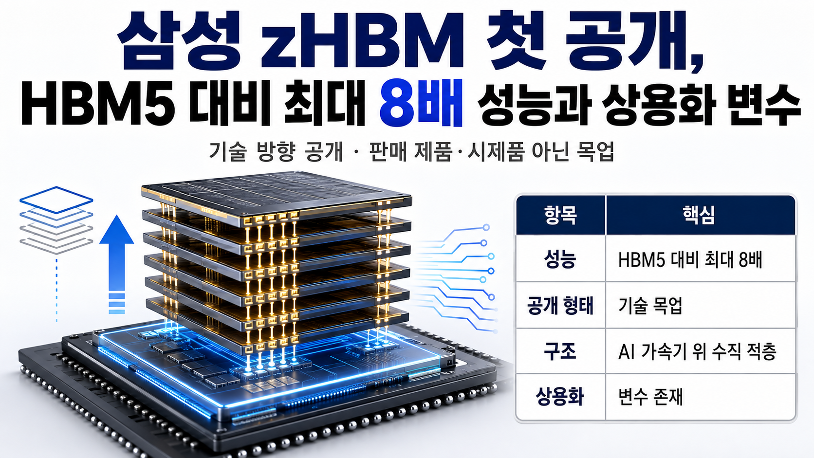
Samsung Electronics has unveiled 'zHBM,' a next-generation 3D memory architecture that vertically stacks HBM on top of an AI accelerator, for the first time. Samsung claims up to 8 times the performance of HBM5, but what it unveiled was a mockup illustrating its technological direction, not a commercial product or prototype.
What Is Samsung zHBM?
zHBM is an architecture that vertically stacks high-bandwidth memory (HBM) on top of an AI accelerator rather than positioning it beside the accelerator. Its central objective is to shorten the physical distance between memory and the processing unit, reducing data-transfer bottlenecks and power consumption.
Samsung Electronics unveiled mockups of zHBM and zNAND-O for the first time in the industry at 'FMS 2026,' held in Santa Clara, California, United States.
In conventional HBM systems, GPUs or other AI accelerators and HBM are positioned side by side on a substrate. Even when the components are connected through high-speed interfaces, limitations remain in the distance data must travel and the interconnection architecture.
zHBM replaces this horizontal arrangement with a vertical architecture.
Conventional HBM: Memory positioned beside the AI accelerator
zHBM: Memory stacked on top of the AI accelerator
Expected benefits: Shorter data-transfer distances, greater bandwidth, and improved power efficiency
Intended applications: Better training and inference performance for large-scale AI models
An 'interlayer' sits between the AI accelerator and HBM. This intermediate semiconductor layer connects signals between the two chips and can incorporate additional functions.
Samsung explained that customer-specific intellectual property (IP) can be incorporated into the interlayer to increase memory capacity or enhance particular functions of an AI accelerator.
What Does 'Up to 8 Times Faster Than HBM5' Actually Mean?
The maximum 8-times figure presented by Samsung represents projected performance for a next-generation interface system incorporating zHBM compared with HBM5. It should not be interpreted as the result of independent benchmark testing of completed commercial products under identical conditions.
| Comparison Metric | HBM5 Baseline | Samsung's Claimed zHBM Figures |
|---|---|---|
| System performance | 1 | Up to 8 times |
| Performance per watt | 1 | Up to 3 times |
| Memory density | 1 | More than 10 times |
| Thermal resistance | 1 | Less than half |
| Development stage disclosed | Next-generation HBM mockup | 3D architecture mockup |
The phrase 'up to' is also important. It does not mean that processing speeds will uniformly increase by 8 times across all AI models and data centers.
Actual performance may vary depending on the AI accelerator architecture, memory capacity, interface, cooling method, software optimization, and AI model being processed.
Converting the Announced Multipliers Into Percentage Changes
If Samsung's announced multipliers are converted using 1 as the baseline value for HBM5, the results are as follows.
Performance at 8 times: An increase of up to 700%
Performance per watt at 3 times: An increase of up to 200%
Memory density exceeding 10 times: An increase exceeding 900%
Thermal resistance below half: A reduction exceeding 50%
These percentage changes are the author's calculations based on the multipliers announced by Samsung Electronics.
The calculation involves 'subtracting 1 from the multiplier and then multiplying by 100.' For example, 8 times corresponds to an increase of `(8-1)×100=700%`.
However, performance, memory density, and power efficiency are different metrics. These figures cannot simply be added together or multiplied to calculate the actual speed improvement of an AI service.
Why Stack Memory on Top of an AI Accelerator?
Even as AI semiconductor processing capabilities improve, accelerators may spend more time waiting if memory cannot supply data quickly enough. This situation, in which data delivery speed limits processing performance, is known as a memory bottleneck or memory wall.
HBM increases bandwidth by vertically stacking multiple DRAM chips, but HBM stacks and AI accelerators are still generally connected side by side on a substrate.
zHBM goes beyond stacking DRAM chips within HBM by moving the entire HBM stack above the AI accelerator. This approach aims to reduce interconnection distances by combining memory and processing components into a single vertical system.
If the architecture is implemented as planned, several changes are expected.
First, more memory could be accommodated within a limited package area.
Second, shorter data-transfer distances could create opportunities to increase bandwidth and improve power efficiency.
Third, it could become easier to customize memory capacity and interconnection functions for a customer's AI processor.
Could Heat Generation Actually Become a Bigger Problem?
Stacking memory above an AI accelerator shortens data-transfer distances, but it may also increase heat concentration. This is why cooling and heat dissipation are just as important as performance in 3D stacking technology.
Samsung stated that applying next-generation wafer bonding technology could reduce thermal resistance by more than half compared with HBM5. Thermal resistance indicates how effectively heat can escape from inside a semiconductor. A lower value means heat can dissipate more easily.
However, the materials released this time did not include operating temperatures, power consumption, cooling conditions, or extended-load test results for an actual functioning chip.
It is therefore important to distinguish the target for improved thermal resistance from actual cooling performance in data centers. This will need to be verified through future silicon prototypes and customer validation.
Is zHBM Currently Being Manufactured or Sold?
As of 2026-08-05, Samsung zHBM is not a commercial product but a conceptual architecture illustrating the direction of next-generation technology. What Samsung unveiled was a mockup, not a functioning final product.
A mockup is a model created to visually demonstrate a product's structure and appearance. Unveiling a mockup indicates that a company has formally presented its development direction, but it does not mean that product performance validation or preparations for mass production have been completed.
Samsung announced plans to collaborate with customers to optimize the integration of AI processors and memory. However, it has not yet officially disclosed the following information.
Timing for producing zHBM prototypes
Schedule for providing samples to customers
Mass-production timeline
AI accelerators and customers that will adopt the technology
Memory capacity and bandwidth for individual products
Pricing and manufacturing costs
Actual manufacturing yields
Cooling methods and package specifications
Therefore, saying 'Samsung has launched memory that is 8 times faster than HBM5' would misrepresent the technology's development stage.
A more accurate description is: 'Samsung has unveiled the first mockup of its zHBM architecture, which targets up to 8 times the performance of HBM5.'
Why This Announcement Matters
zHBM reflects the view that simply advancing to higher HBM generations may not be enough to meet the demands of future AI systems. It signals intensifying competition to design memory chips, AI accelerators, interfaces, packaging, and cooling as an integrated system.
Samsung is linking its zHBM strategy to its ability to provide memory, system semiconductor design, foundry services, and advanced packaging together.
In particular, the functions that can be incorporated into customer-specific interlayers and whether actual joint design projects proceed with AI accelerator manufacturers will be important indicators of the technology's commercialization potential.
However, the unveiling of a new architecture alone does not establish that supply contracts have been secured or that financial performance will improve. For its technological objectives to translate into actual products, the architecture must meet requirements for manufacturing yield, cost, thermal management, reliability, and customer validation.
Announcements to Watch Next
The real progress of zHBM will become clearer through the stages that follow the mockup announcement.
The first development to watch is whether Samsung unveils a silicon prototype manufactured as an actual semiconductor. Once a prototype is available, specific performance figures can be compared, including memory capacity, bandwidth, power consumption, and cooling conditions.
This should be followed by customer sample shipments, compatibility validation with AI accelerators, and a mass-production schedule.
The relationship between the development and mass-production roadmap for HBM5 and zHBM is also important. The implications for Samsung's product roadmap could differ depending on whether zHBM is a separate memory product intended to replace HBM5 directly or a system architecture that vertically integrates HBM5.
Based solely on the information disclosed as of 2026-08-05, zHBM is closer to Samsung's proposed direction for next-generation AI memory design than to a finished product approaching commercial launch.
More important than the headline figure of up to 8 times the performance are the actual prototype, customer validation, and mass-production timeline. Only when these three stages are disclosed will it be possible to assess whether zHBM's technological objectives can translate into real-world performance improvements in commercial data centers.